NSOM FLIM with the Nanonics AFM/NSOM System
Wolfgang Becker, Becker & Hickl GmbH
Yaakov Tischler,
Bar Ilan University
Abstract: We present an NSOM FLIM system based on the AFM/NSOM system of
Nanonics Imaging, Jerusalem, and a Simple-Tau 150 TCSPC FLIM system of
Becker & Hickl, Berlin. The system is able to record FLIM data at high
pixel numbers, and with a full fluorescence decay function in each pixel. We
demonstrate the system for recording FLIM of nano-islands on a semiconductor
surface.
Principle
The scanning near-field optical microscope
(SNOM or NSOM) combines the principles of the atomic force microscope (AFM) and
the laser scanning microscope [9]. A sharp tip is scanned over the sample
and kept in a distance comparable to the diameter of a single molecule. The tip
can be the end of a tapered fibre through which the laser is fed to the sample,
see Fig. 1, left. Or, a metallic tip is illuminated by focusing the laser
through the microscope objective on it. The evanescent field at the tip is used
to probe the sample structure (Fig. 1, right). In both cases the fluorescence
photons are collected through the microscope objective lens. Scanning is performed
by moving the sample by a piezo-driven scan stage.
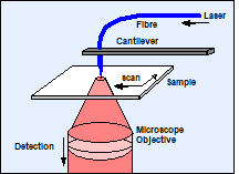
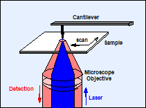
Fig. 1: Optical near-field microscope: Left: Tapered fibre configuration.
Right: Tip enhancement configuration.
The NSOM principle combines nanometer-scale
topography information from the AFM with spectroscopic information from the
optical detection.
Because NSOM uses a scanning principle it
can easily be combined with TCSPC FLIM. Early implementations data back to 2003
and 2004 [10, 11]. All that is required for FLIM is an output of the
synchroninisation pulses (start-of-frame,
start-of-line, start-of-pixel) from the piezo
controller, an optical input for a pulsed laser, and an optical output to a single-photon
detector.
Nanonics AFM / NSOM System
For the experiments described here we used
the AFM/NSOM system of Nanonics Imaging Ltd., Jerusalem [13]. The system is
shown in Fig. 2, left, the scan stage with the AFM tips in Fig. 2, right.
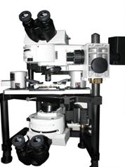
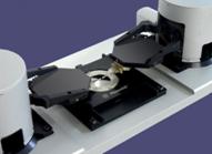
Fig. 2: Left:
Photo of Nanonics system. Right: Sample scanning stage
with AFM tips
The system we used for FLIM is based on a
double microscope, see Fig. 2, left. Both the excitation and the detection can
be performed from the top or from the bottom of the sample. The system can be
used both in the tip enhancement and in the tapered fibre configuration.
To obtain AFM and NSOM images, the sample
is placed on a three-axis piezo stage (Fig. 2, right). The piezo stage is used
both for keeping the AFM probe at a constant distance to the sample surface,
and for raster scanning in x and y. The images presented below were collected
in the tapered-fibre configuration.
FLIM System
For fluorescence lifetime imaging, the Nanonics
system was combined with a bh BDL‑SMN 488 nm picosecond diode laser
[2], a bh Simple-Tau 150 TCSPC FLIM system [2], and a bh HPM‑100-40 GaAsP
hybrid detector [2, 4]. The system components are shown in Fig. 3.
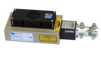
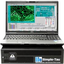
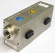
Fig. 3: Components of the FLIM system. Left to right: BDL‑SMN ps
diode laser, Simple-Tau 150 TCSPC FLIM system, HPM‑100-40 hybrid
detector.
The BDL‑SMC laser generates pulses of
488 nm wavelength, 50 ps pulse duration, and 80, 50, or 20 MHz repetition
rate. Other wavelengths are available, see [3]. The laser has a beam-profile
corrector and a Qioptiq single-mode fibre connector. The power injected into
the fibre is about 2 mW at 80 MHz. Higher power is available if an
increase of the pulse duration is acceptable [3].
The Simple-Tau 150 consists of a
laptop computer with a bus extension cable and an electronics box. The box
contains a bh SPC‑150 TCSPC/FLIM module and a DCC‑100 detector
controller. The HPM‑100 detector contains a Hamamatsu R10467-40 hybrid
PMT tube, the high-voltage generators for the operating voltages of the R10467-40
tube, and a GHz-bandwidth low-noise preamplifier. The detector has a detection
efficiency of about 50% and is free of afterpulsing. The result is a very good
photon efficiency of the FLIM measurement: The number of photons required to
reach a given lifetime accuracy is very close to the ideal value [2].
Fluorescence lifetime imaging in the SPC‑150
TCSPC card is based on a multi-dimensional TCSPC process [1, 2]. The principle
is shown in Fig. 4, left. The TCSPC module receives the single-photon pulses
from the detector, the timing reference pulses from the laser, and the scan
synchronisation pulses (start-of-frame, start-of-line, start-of-pixel) from the
scan controller of the Nanonics system. For every photon, the TCSPC system
determines the time, t, in the laser pulse period, and the location (x, y, of
the AFM tip) in the scan area. From these pieces of information, the TCSPC
process builds up a photon distribution over x, y, and t. The distribution can
be interpreted as an array of pixels over x and y, each containing a full
fluorescence decay function over the time in the pulse period, t. The advantage
of the process is that it records a full fluorescence decay function in each
pixel, not only a fluorescence lifetime. Moreover, it records at near-ideal
photon efficiency, and it can be used at any scan rate. In laser scanning
microscopes (with scan rates on the order of 106 pixels per second)
the acquisition is run over a larger number of frames. At the slow scan rates
used in AFM / NSOM the data are usually acquired over a single frame. The
result is independent of the scan rate if the total acquisition time and the
detection rate are the same [2].
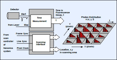
Fig. 4:
Principle of TCSPC FLIM
The SPC‑150 module in combination
with bh 64 bit SPCM data acquisition software is able to record images of
megapixel size [2, 12]. This makes the FLIM system compatible with the high
pixel numbers often used in AFM. Frames sizes of 2048 x 2048 pixels,
1024 x 1024 pixels, and 512 x 512 pixels are possible at a time
resolution of 256, 1024, and 4096 time channels per pixel, respectively [2].
The high number of time channels can be useful when NSOM decay data contain
both very fast and very slow decay components.
All data presented here were recorded by
the principle described above, and in the FIFO Imaging mode of the SPCM data
acquisition software. FLIM data analysis was performed by bh SPCImage FLIM data
processing software [2].
Results
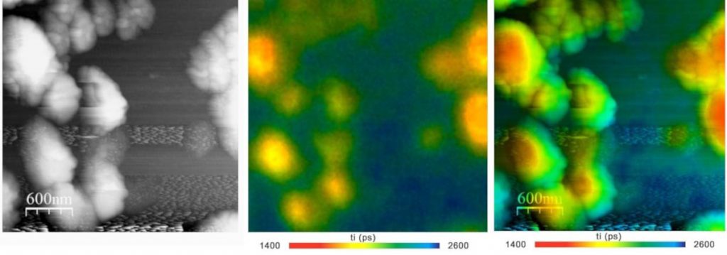
Fig. 5 shows nano islands of fluorescing
material on a semiconductor surface. The AFM image is shown left, the FLIM
image in the middle. The right image is a combination of the AFM data with the
fluorescence lifetime data.
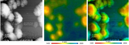
Fig. 5: NSOM FLIM of nano-islands on a semiconductor surface. Left:
Topography from AFM system. Middle: FLIM. Right: Overlay of AFM topography
image with lifetime from FLIM. Amplitude-weighted lifetime of double-exponential
decay. Nanonics AFM / NSOM system with bh SPC‑150 FLIM system and BDL‑SMN
488nm ps diode laser. Data courtesy of Yaakov Tischler, Bar Ilan University.
Summary
NSOM systems can easily by combined with bh
FLIM systems if they provide an output for the synchroninisation pulses from
the piezo controller, an optical input from a pulsed laser, and an optical
output to a photon counting detector. These requirements are met by the
Nanonics AFM/NSOM systems. We tested a combination of this sysem with a bh
Simple-Tau 150 TCSPC FLIM system, a bh BDL-SMN ps diode laser, and a bh
PMH-100-40 hybrid detector. The advantage of NSOM FLIM is that both
high-resolution topography data and fluorescence lifetime data are obtained.
The data can be combined into images that show the topography as brightness and
the fluorescence lifetime as colour. The technique described can be extended to
combined fluorescence/phosphorescence lifetime imaging [5], laser wavelength multiplexing [2], multi-wavelength detection [2, 7], and NIR detection [8].
References
1. W. Becker, Advanced time-correlated single-photon counting
techniques, Springer (2005)
2.
W. Becker, The bh TCSPC handbook. Becker &
Hickl GmbH, 6th Edition (2015), www.becker-hickl.com, printed copies available from bh
3. Becker & Hickl GmbH, BDL-SMN series picosecond diode lasers.
User handbook, www.becker-hickl.com
4.
Becker, W., Su, B., Weisshart, K. & Holub,
O. (2011) FLIM and FCS Detection in Laser-Scanning Microscopes: Increased
Efficiency by GaAsP Hybrid Detectors. Micr. Res. Tech. 74, 804-811
5.
Becker, W., Su, B., Bergmann, A., Weisshart, K.
& Holub, O. (2011) Simultaneous Fluorescence and Phosphorescence Lifetime
Imaging. Proc. SPIE 7903, 790320
6.
Becker, W., Su, B., Bergmann, A., Weisshart, K.
& Holub, O. (2011) Simultaneous Fluorescence and Phosphorescence Lifetime
Imaging. Proc. SPIE 7903, 790320
7. Becker & Hickl GmbH, MWFLIM GaAsP multi-spectral FLIM detectors.
Data sheet, www.becker-hickl.com
8. W. Becker, V. Shcheslavskiy, Fluorescence Lifetime Imaging with
Near-Infrared Dyes. Proc. SPIE 8588 (2013)
9.
R.C. Dunn, Near-field scanning optical microscopy,
Chem. Rev. 99, 2891-2927 (1999)
10. D. Hu, M. Micic, N. Klymyshyn, Y.D. Suh, H.P. Lu, Correlated
topographic and spectroscopic imaging beyond diffraction limit by atomic force
microscopy metallic tip-enhanced near-field fluorescence lifetime microscopy,
Rev. Sci. Instrum. 74, 3347-3355 (2003)
11. M. Micic, D. Hu, Y.D. Suh, G. Newton, M. Romine, H.P. Lu, Correlated
atomic force microscopy and fluorescence lifetime imaging of live bacterial
cells, Colloids and Surfaces B, Biointerfaces 34, 205-212 (2004)
12. Studier, H., Becker, W. Megapixel FLIM. Proc. SPIE 8948, (2014)
13. www.nanonics.co.il
Contact: Wolfgang
Becker, becker@becker-hickl.com