The PZ-FLIM-110
Piezo-Scanning FLIM System
Wolfgang Becker,
Holger Netz, Becker & Hickl GmbH, Berlin, Germany
Abstract. The
PZ‑FLIM-110 Piezo Scanning FLIM system uses bhs multi-dimensional TCSPC
technique in combination with a piezo scanner. The scanner is controlled via a
bh GVD-120 scanner control card, the FLIM data are recorded by an SPC-150 or
SPC-160 TCSPC / FLIM module. Data acquisition is controlled by 64 bit
bh SPCM TCSPC software. The system is able to run X-Y scans, X-Z (vertical) scans,
and to record simultaneously FLIM and PLIM data. Maximum FLIM data formats are
512 x 512 pixels, 4096 time channels, or 2048 x 2048
pixels, 256 time channels.
Stage Scanning
TCSPC FLIM systems use a combination of
multi-dimensional TCSPC with optical scanning. TCSPC records fluorescence decay
data at extremely good temporal resolution [1, 5, 6], near-ideal photon efficiency, and
with the capability to resolve multi-exponential decay profiles into individual
decay components [3]. Optical scanning delivers images that are free of
out-of-focus haze and free of lateral and longitudinal scattering. TCSPC FLIM
thus combines the most accurate and efficient electronic technique of
fluorescence decay recording with the most accurate optical imaging technique [5].
Optical scanning for FLIM is normally
performed by galvanometer scanners in combination with confocal detection or
multiphoton excitation [5]. The
high scan rate obtained by these systems is no problem for TCSPC FLIM. On the
contrary, it the basis of advanced techniques like fast time-series recording [12],
temporal mosaic imaging [11],
and FLITS [4]. Moreover, it is required to run fast preview scans for selecting
the desired focal plane, scan area, and sample position [6, 7].
Instead of scanning the laser and detection
light beam the sample can be moved by a piezo scan stage. Sample scanning was
used in the first confocal systems introduced by Marvin Minsky [13]. Moving the
sample has the advantage that the optical system always works on the optical
axis, and that the image area is not limited by the field of view of the
microscope lens. Thus, high-NA lenses with high optical resolution and high
light-collection efficiency can by used for imaging of large fields of view.
However, sample scanning has serious
drawbacks. The most obvious one is that sample scanning is very slow. Typical
scan rates are on the order of one to five lines per second, compared to 1000
lines per second for a galvanometer scanner. Another problem is that the
scanning exerts forces on the sample. This is not acceptable for live-cell
imaging. Nevertheless, sample scanning is often considered a cost-efficient
alternative to beam scanning. This application note shows how sample scanning
is integrated into the bh FLIM hardware and software.
Optical Principle
Two optical principles of a confocal system
with sample scanning are shown in Fig. 1.
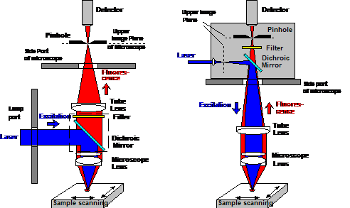
Fig. 1: Optical principle of a sample
scanning system with confocal detection. Left: Beamsplitter and emission filter
in microscope beamsplitter cube, pinhole and detector attached to the side port
of the microscope. Right: Beamsplitter filter, pinhole and detector in compact
optical assembly attached to a side port of the microscope.
A frequently used configuration is shown in
Fig. 1, left. The laser beam is injected into the microscope
via the lamp port of the microscope. The beamsplitter and the emission filter
are inserted in one of the standard microscope filter cubes in the filter
carousel of the microscope. The detector is attached to a side port of the
microscope. A pinhole in the upper image plane of the microscope suppresses
out-of-focus light. The setup is easy to implement but has serious
disadvantages: The lamp port cannot be used for a fluorescence lamp, and the
laser beam diameter must be increased to match the size of the back aperture of
the microscope lens. The most significant problem is alignment. The laser must
be focus in the sample must conjugate exactly with the pinhole. The angle of
the dichroic mirror in the filter cube is therefore critical. Microscopy filter
cubes are not designed for this level of precision. The setup is therefore not
suitable for high-resolution confocal imaging.
The system in Fig. 1, right, has the laser
input, the dichroic beamsplitter, the emission filter, the pinhole, and the
detector integrated in one and the same compact optical building block. The
entire block is attached to an optical port of the microscope. By placing the laser
input, the dichroic mirror, and the pinhole on the same solid mechanical support
the system stays in alignment much better than the system shown in Fig. 1,
left. Further improvement in alignment stability can by achieved by
fibre-coupling the laser and the detector. A problem of the setup can, however,
arise from the fact that the upper image plane of the microscope is close to
the side port. The dichroic mirror and the filter then do not fit between the
port and the image plane.
The optical system available from bh therefore
uses the setup shown in Fig. 2. A ps diode laser (bh BDL or BDS series [9, 10]) is coupled into the system via a
single-mode fibre. A Qioptics (formerly Point-Source) fibre collimator is used
to obtain a collimated beam out of the fibre. The beam is reflected down into
the microscope beam path by a dichroic mirror. L1 focuses the laser into the
upper image plane of the microscope. The laser thus forms a focused spot in the
sample. The fluorescence light from the sample is collected back through the
microscope lens, collimated by L1, and separated from the laser beam by the
dichroic mirror. A bandpass or longpass filter in the collimated beam selects
the detection wavelength range. The light passing the filter is focused into a
multi-mode fibre by a second lens, L2. The core of the fibre forms the
confocal pinhole. The light collected by the fibre is transferred to the
detector.
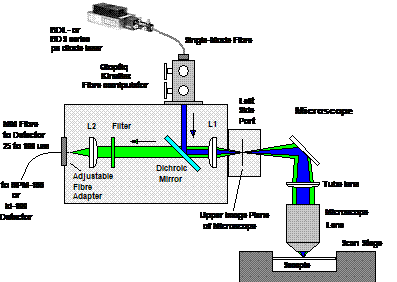
Fig. 2:
Optical principle of the PZ-FLIM piezo stage scanning system. Beam path and optical elements not to
scale.
Control of the Scan Stage
The scan stage is controlled by a bh
GVD-120 scan controller card [6], see Fig. 3. The GVD-120 runs a linear raster
scan in X and Y at a maximum resolution of 2048 x 2048 pixels. The
x-y signals are generated by the hardware of the GVD module, the software is
only used to load different waveforms or scan parameters in the scan
controller. The waveforms are therefore independent of the computer speed and
of software reaction times. The DCS‑120 uses a cycloid trajectory for the
fly-back of the scanner (see Fig. 3, right). This minimises mechanical
resonances, and thus allows the scanner to be operated at the maximum possible
line rate. Moreover, it minimises acceleration forces in the sample. The GVD‑120
also generates the scan synchronisation pulses for bh TCSPC modules, and the
beam blanking, multiplexing, and intensity control signals for two bh BDL-SMC,
BDL‑SMN, or BDS-SM ps diode lasers. The control of the GVD card is fully
integrated in the SPCM software of the bh TCSPC systems [6, 7].
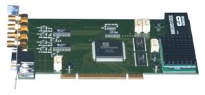
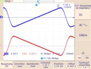
Fig. 3: GVD‑120
scan controller card (left) an scan waveforms (right)
The GVD‑120 scanner control panel of
the SPCM software is shown in Fig. 4, left. The scan is started or stopped by
the Start Scan and Stop Scan buttons at the upper left. Frame and line
scans of different pixel numbers are defined via the Scan field and the
Frame Size field. The scan speed is either selected via a slider, or the
speed is automatically set to the maximum possible scan rate for the scan
amplitude used. The Scan area is either defined by the Zoom and Offset
sliders, or by moving the scan area in a symbolic field of view. A point
measurement is defined by clicking on the Park Beam button. The beam park
position can be defined in a previously recorded FLIM image, please see please
see [6] or [7] for details.
The GVD-120 also controls two bh ps diode
lasers. The laser on/off buttons and the laser power sliders are on the upper
right. Beam blanking during the line and frame flyback is available to reduce
photobleaching. The two lasers can be multiplexed synchronously with the pixels,
lines, or frames of the scan. The multiplexing function is also used for
phosphorescence lifetime imaging by bhs dual-time base PLIM technique [2, 6, 7].
For operation with a scan stage, the
GVD-120 hardware parameters can be adapted to scanners of different speed via
the GVD Adjustment parameters shown in Fig. 4, right. For details please see
[6] or [7].
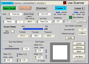
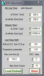
Fig. 4: Scanner control panel of the
SPCM software (left) and setup of the scan speed parameters (right)
TCSPC Recording
TCSPC FLIM data are recorded by bhs
multi-dimensional TCSPC process [1, 5, 6]. Single photons of the fluorescence
light are detected, the detection time, t, within the laser pulse period and
the position of the laser beam in the sample in the moment of the photon
detetction, x,y, are determined, and a photon distribution is built up over
x,y,t. The result is an array of pixels with a full fluorescence decay curve in
each pixel. With 64 bit SPCM software FLIM data formats of up to
2048 x 2048 pixels and 256 time channels can be used [8, 14]. Other
formats can be defined, such as 512 x 512 pixels with up to 4096 time
channels. Please see [6] for details.
System Architecture
The basic system architecture of a GVD‑120-based
piezo scanning system is shown in Fig. 5. The simplest system consists of an
SPC-150, 160, or 830 TCSPC module, a GVD-120 scan control card, a piezo stage,
a BDL or BDS series ps diode laser, and a Id Quantique, id100-50FP fibre
coupled SPAD detector, see Fig. 5, left. Alternatively, an HPM-100-40 or -50
hybrid detector can be used. The HPM‑100 is controlled by a DCC-100 detector
controller card, see Fig. 5, right.
The ramp voltages generated by the GVD‑120
scan controller are connected to the driver amplifier of the piezo stage as
shown in Fig. 5.
The signal acquisition in the TCSPC board
is synchronised with the scanning via frame, line, and pixel clock pulses
generated by the GVD‑120 card as usual [6, 7]. The scan clock pulses are connected
to the 15 pin connector of the TCSPC module. The GVD‑120 also
controls the ps diode laser.
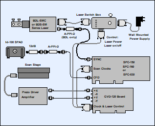
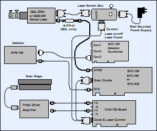
Fig. 5: Piezo stage scanning system
controlled by the bh GVD‑120 board. Left: With
id100-50 SPAD detector. Right: With HPM‑100 hybrid detector.
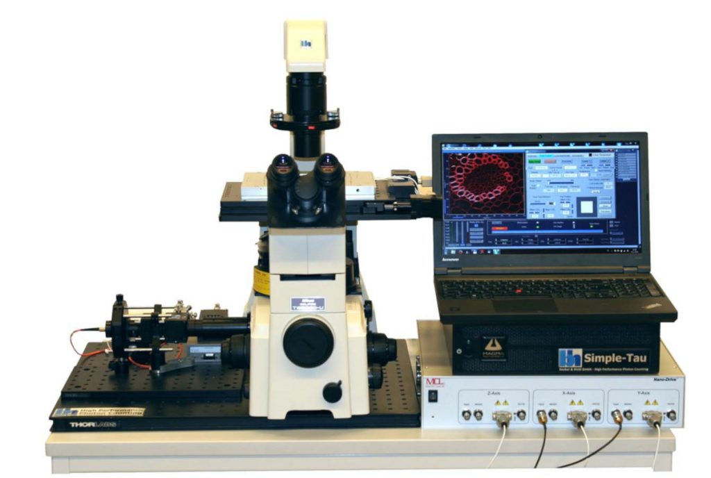
A photo of the entire piezo scanning system
is shown in Fig. 6. It consists of a Nikon TE2000 microscope, a PZ-FLIM optical
assembly connected to left side port, a BDL-SMN ps diode laser, a Mad City Labs
Nano-View 200-3 piezo system, and a bh Simple-Tau TCSPC system. Other
microscopes can be used if a side port is available.
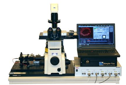
Fig. 6: Photo of the bh PZ-FLIM-110 piezo scanning system. Nikon TE2000 microscope, PZ-FLIM optical
assembly connected to left side port, BDL-SMN ps diode laser, Mad City Labs Nano-View 200-3
piezo system, bh Simple-Tau TCSPC system.
Results
X-Y FLIM (Lateral Scan)
For recording the images shown below we used
the system shown in Fig. 6, with a Mad-City-Labs Nano-View 200-3 piezo
stage. (For an example with a PI scan stage please see [6]). A typical
fluorescence lifetime image of a convallaria sample is shown in Fig. 7.
Scanning was performed at a resolution of 512 x 512 pixels, and at a
rate of 1 line, or 512 pixels, per second. The decay data were recorded at a
temporal resolution of 1024 time channels, corresponding to 12.2 ps per time
channel. Please note that up to 4096 time channels can be used without the need
of decreasing the pixel number or compromising the recording speed or
efficiency [6, 14]. The average count rate over the entire sample was 106
photons per second, corresponding to about 5×10⁶ photons per
second in the brightest pixels. The microscope lens was a Nikon 40x, NA=1.3 S Fluor
oil immersion lens. The diameter of the detection fibre was 50 µm,
corresponding to a pinhole diameter of about 3 Airy disk diameters, or
3 AU (Airy Units).
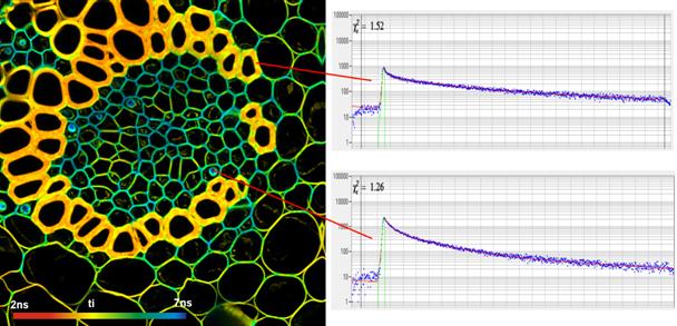
Fig. 7: Lifetime image of a convallaria sample. Intensity-weighted
lifetime of triple-exponential decay. 512 x 512 pixels, 1024 time
channels per pixel. 40x NA1.3 Oil immersion lens, effective pinhole size 3
AU. Right: Decay curves in selected pixels
The data shown in Fig. 7 feature high
spatial resolution and clean decay data in the individual pixels. The problem
is, as for any stage scanning system, the long acquisition time. Unless a
substantial fraction of the line time is sacrificed for the line flyback the
scanner cannot be run much faster than 5 lines per second. An image of
512 x 512 pixels therefore requires a scan time of at least 100 seconds.
Recording an image of 2048 x 2048 pixels - easily achieved with the
DCS‑120 galvanometer scanning system [7, 14] - would require about 400 seconds, or
6.6 minutes. Such long acquisition times may be acceptable for acquisition of
ultra-high quality decay data. In that case, the acquisition time is determined
rather by the time required to record enough photons in the individual pixels
than by the scan time. For standard FLIM applications the scan times are inconveniently
long, and for time-series recording they are clearly unacceptable. The biggest
problem caused by the long scan time is the impossibility of accurate focusing.
Fine focusing, i.e. selection of the desired image plane within the
longitudinal dimension of the sample, has to be done on the basis of confocal
images. Even a perfectly parfocal eyepiece or camera does not solve the problem
- the features to be imaged by confocal scanning may simply not be visible this
way. This is especially the case in thick samples of biological tissue with strong
longitudinal and lateral scattering [5].
X-Z FLIM (Vertical Scanning)
The piezo system used for the experiments
described here has a third axis which can be used to scan the sample vertically.
All that has to be done to obtain a vertical scan is to swap the Y output from
the GCD-120 from the Y input of the piezo amplifier to the Z input. A x-z scan (vertical
scan) of the convallaria sample is shown in Fig. 8.
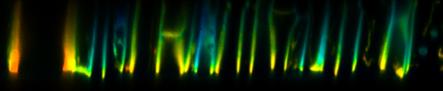
Fig. 8:
Vertical (x-z) scan through a convallaria sample. Horizontal scan range
100 µm, vertical scan range 25 µm
For vertical scanning the speed
disadvantage of piezo scanning compared with galvanometer scanning is less
significat than for x-y scanning. What ever the line rate is - the time
required for one Z step is determined by the speed of the Z drive. The Z drive
is either the Z drive of a microscope or a piezo element and thus not faster
than a few 10 ms per step. Also the focusing problem is less sinificant. The
start position of the Z scan need not be defined as accurately as the image
plane of an X-Y scan.
PLIM
In 2011 bh introduced a combined FLIM /
PLIM techniques that is based on an additional on/off modulation of a pulsed
laser, and recording photon times both within the laser pulse period and the
laser modulation period [2]. In other words, the PLIM signal is excited by many
laser pulses, not only by a single one. The result is a dramatic increase in
PLIM sensitivity, and the possibility to record FLIM and PLIM simultaneously in
the same scan. An example of a PLIM measurement with a palladium dye is shown
in Fig. 9.
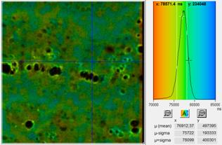
Fig. 9: PLIM
measurement of a palladium dye. Phosphorescence lifetime image, histogram of
lifetime over the pixels, decay curve in selected spot. 1024 time channels, time
scale 1.3 ms. Decay time is 79 µs.
For PLIM or combined FLIM/PLIM the speed
disadvantage of the piezo scanner is less significant than for FLIM. The pixel
time of the scan must be selected a few times longer than the phosphorescence
lifetime, which means a slow scan has to be used. Phosphorescence lifetimes are
often on the order of 50 µs (for platinum dyes) or a few 100 µs (for
palladium dyes), which means pixel dwell times on the order of 200 µs or
2 ms, respectively. This is close to or even within the reach of a piezo
scanner.
Summary
The PZ-FLIM-110 Piezo-Scanning FLIM system
records X-Y scans and X-Z scans of FLIM and FLIM/PLIM data at excellent spatial
and temporal resolution. Problems do, however, arise from the slow scan speed
of the piezo stage. Under typical imaging conditions, the acquisition time is
determined by the speed of the scanner, not by the time needed to acquire the
desired number of photons. Scan times for 512 x 512 pixel images are
on the order of 100 seconds, scan times for 2048 x 2048 pixel images are
at least 6.6 minutes. These scan times may be acceptable for high quality FLIM
but not for imaging dynamic effects in a life sample. Moreover, the slow scan
rate makes focusing into a defined image plane within a sample difficult. If
these restrictions are taken into account the PZ‑FLIM-110 is a cost-efficient alternative to a DCS‑120 galvanometer
scanner system.
References
1. W. Becker, Advanced time-correlated single-photon counting techniques. Springer, Berlin, Heidelberg, New York, 2005
2.
W. Becker, B. Su, A. Bergmann, K. Weisshart, O.
Holub, Simultaneous Fluorescence and Phosphorescence Lifetime Imaging. Proc.
SPIE 7903, 790320 (2011)
3. W. Becker, Fluorescence Lifetime Imaging - Techniques and
Applications. J. Microsc. 247 (2) (2012)
4. W. Becker, V. Shcheslavkiy, S. Frere, I. Slutsky, Spatially Resolved Recording of Transient Fluorescence-Lifetime
Effects by Line-Scanning TCSPC. Microsc. Res. Techn. 77, 216-224 (2014)
5. W. Becker (ed.), Advanced time-correlated single photon counting
applications. Springer, Berlin, Heidelberg, New York (2015)
6. W. Becker, The bh TCSPC handbook. 6th. edition, Becker & Hickl
GmbH (2015), printed copies available from bh, electronic version available on www.becker-hickl.com
7.
Becker & Hickl GmbH, DCS-120 Confocal
Scanning FLIM Systems, user handbook, 6th edtion Becker
& Hickl GmbH (2015), printed copies available from bh, electronic version
available on www.becker-hickl.com
8. Becker & Hickl GmbH, Megapixel FLIM with bh TCSPC Modules: The
New SPCM 64-bit Software. Application note, available on www.becker-hickl.com
9. Becker & Hickl GmbH, BDL-SMN series picosecond diode lasers. User
handbook, available on www.becker-hickl.com
10. Becker
& Hickl GmbH, BDS series picosecond diode lasers. Extended data sheet,
available on www.becker-hickl.com
11. Becker
& Hickl GmbH, bh FLIM Systems Record Calcium Transients in Live Neurons.
Application note, available on www.becker-hickl.com
12. V.
Katsoulidou, A. Bergmann, W. Becker, How fast can TCSPC FLIM be made? Proc.
SPIE 6771, 67710B-1 to 67710B-7 (2007)
13. M. Minsky, Memoir on inventing the confocal microscope, Scanning 10,
128-138 (1988)
14. H.
Studier, W. Becker, Megapixel FLIM. Proc. SPIE 8948 (2014)