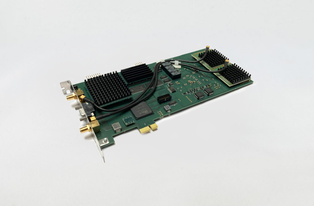
- High-Throughput PCIe Interface
- SPC-180N Technology
- Unprecedented Timing Stability and Time Resolution
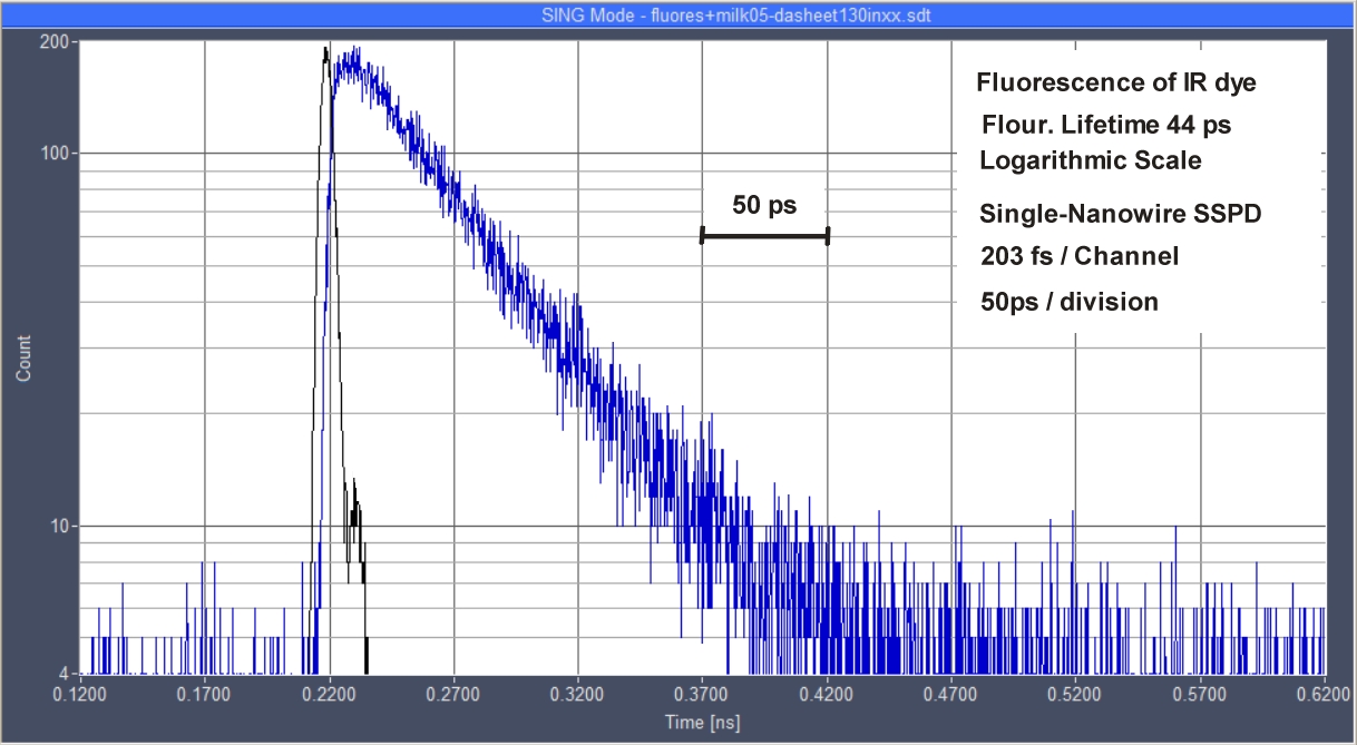
- Time Channel Width Down to 203 fs
- Internal Timing Jitter (RMS) / IRF Width (FWHM) Down to 1.1 ps / 2.8 ps
- 12 MHz Saturated Count Rate
- -NX and -NXX Versions Ideal for Ultra-Fast HPM (Hybrid) Detectors and Superconducting NbN Detectors
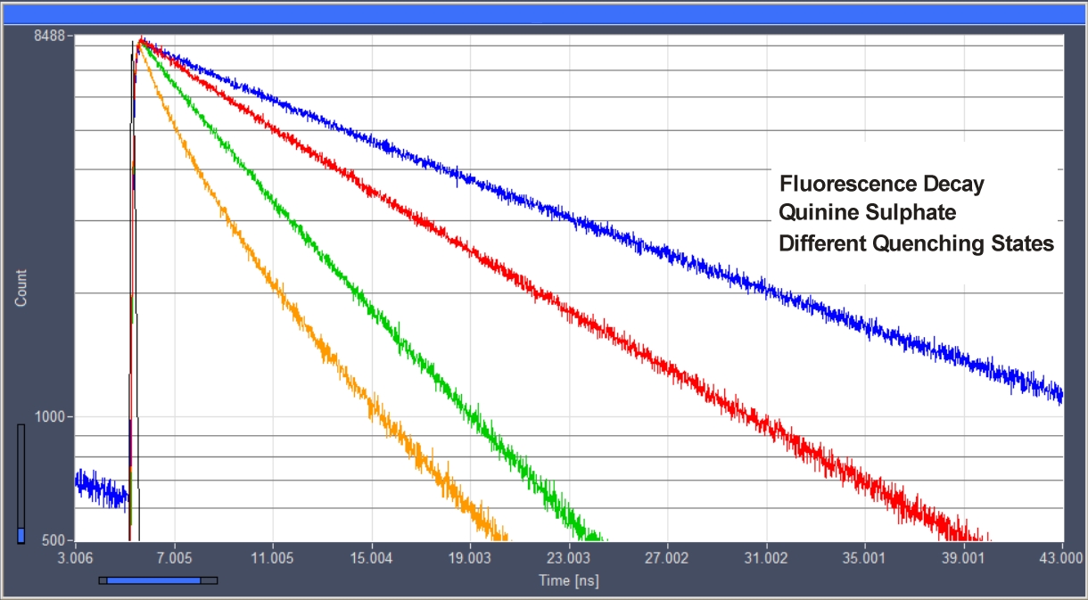
- Precision Fluorescence Decay Recording
- Simultaneous Fluorescence / Phosphorescence Decay Measurement
- Multi-Wavelength Fluorescence Decay Measurement
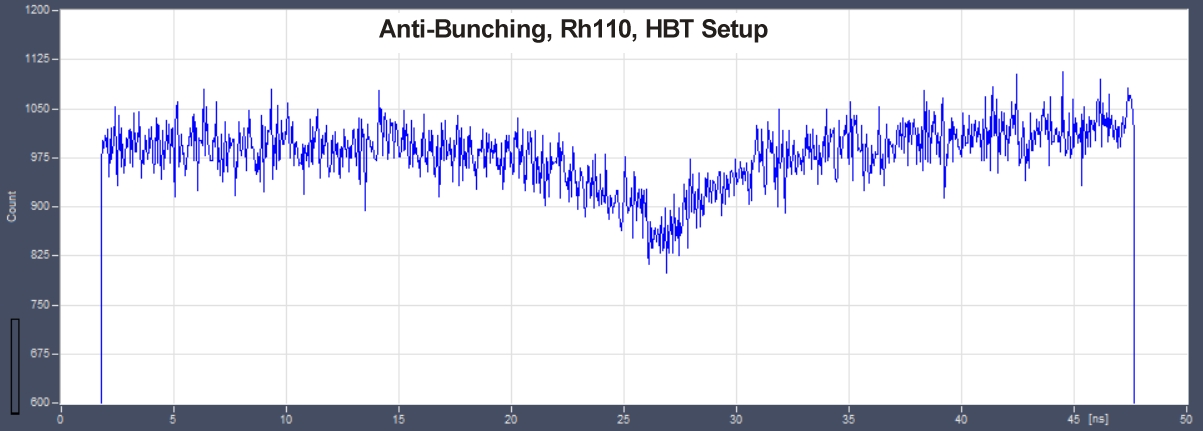
- Photon Correlation, Single-Molecule Spectroscopy
- Free Instrument Software for Windows 10 / 11
- Realtime Calculation and Fitting of FCS Curves
- Link to SPCImage NG Data Analysis
- Parallel Operation of Up to 4 Modules
- Available as Multi-Module Package e.g. SPC-132IN, SPC-133IN and SPC-134IN
Description
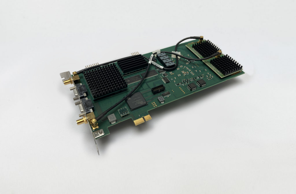
The SPC-130IN is a high-end performance single photon counting (TCSPC) module with high time resolution down to the ps range at affordable costs. The timing module is the ideal choice for fluorescence lifetime applications and time correlation recording, with highest accuracy providing precise time information.
General Information
The module is available in three versions with different time range and time resolution:
Minimum Time Channel Width
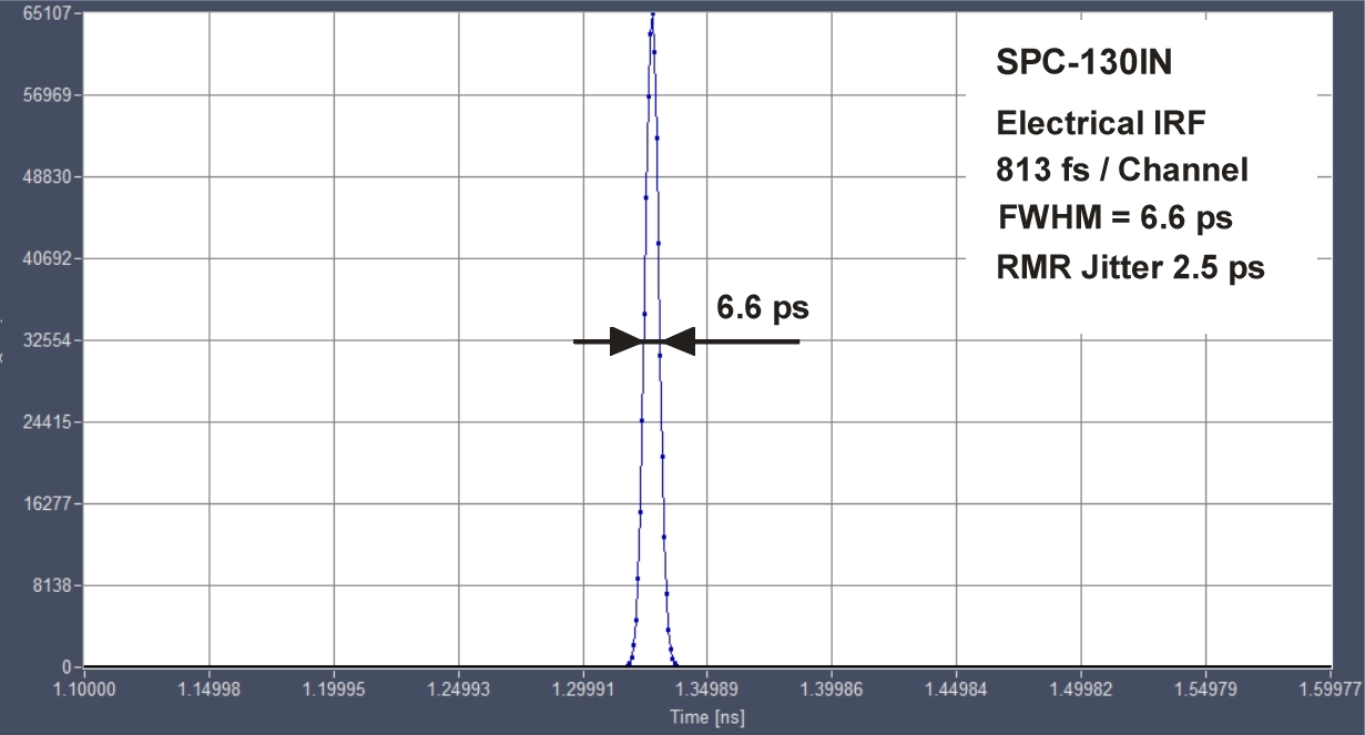
SPC-130IN: 813 fs
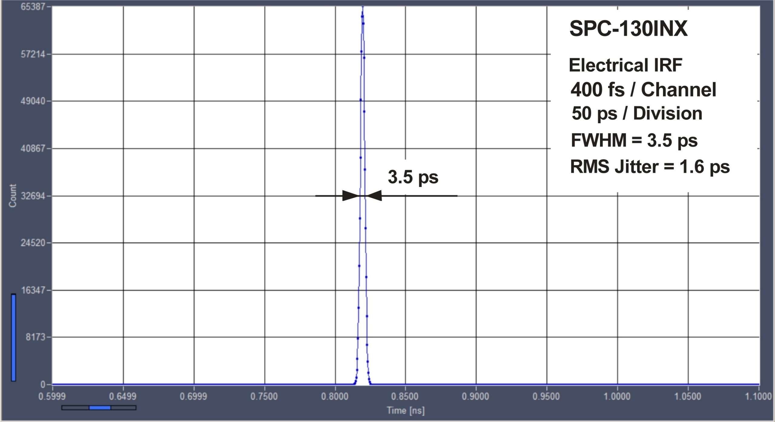
SPC-130INX: 405 fs
SPC-130INXX: 203 fs
Internal Timing Jitter (RMS) / IRF Width (FWHM)
SPC-130IN: 2.5 ps / 6.6 ps
SPC-130INX: 1.6 ps / 3.5 ps
SPC-130INXX: 1.1 ps / 2.8 ps
The -NX version, and, especially, the -NXX version have been designed for ultra-fast detectors, SSPDs and ultra-fast hybrid detectors. The hardware interface achieves extremely high data transfer rates especially in the parameter-tag modes.
The SPC-130IN modules have all standard photon distribution modes, the continuous-flow mode, and the FIFO (time-tag) mode implemented. However, this timing module has no imaging mode. The SPC-130IN can thus be used for traditional fluorescence lifetime experiments, diffuse optical tomography, stopped flow experiments, single molecule detection and combined FCS/lifetime experiments. The SPC-130IN has especially overvoltage-hardened signal inputs. They are reliable and rugged, and can be used even under harsh conditions. When ordered in large quantities for OEM applications, the bh SPC-130IN modules offer unprecedented price-performance ratio. The module is upgradable to SPC-180N for fluorescence lifetime imaging microscopy (FLIM) and other laser scanning applications.
All SPC-130IN family modules have high-speed PCI-Express (PCIe) interfaces and can be easily installed in nearly all PCs or configured as stand-alone timing unit.
Measurement Software Included
The SPCM operating and measurement software is included with all SPC series modules. SPCM provides online calculation and display (2D, 3D) of data (decay curves, FCCS) acquired in multiple operation modes. SPCM software undergoes active continuous development. SPCM receives frequent updates with new features and bug fixes. Read more…
FLIM and FCS Data Analysis
For advanced fluorescence lifetime single-curve data analysis, please use SPCImage.
For advanced visualisation and analysis of dynamic effects, please use SPCDynamics.
For advanced fluorescence correlation spectroscopy (FCS) and cross-correlation (FCCS) data analysis, please use Burst Analyzer.
Custom Programming Libraries (DLL, LabVIEW)
For automation and custom software integration, DLLs and LabVIEW drivers are available. Read more…
Specifications
|
SPC-130IN |
SPC-130INX |
SPC-130INXX |
|
|
Photon Channel |
|
||
|
Principle |
Constant Fraction Discriminator (CFD) |
||
|
Discriminator Input Bandwidth |
4 GHz |
||
|
Time Resolution (FWHM/RMS, electr.) |
< 6.6 ps / 2.5 ps |
< 3.5 ps / 1.6 ps |
< 3 ps / 1.1 ps |
|
Variance in Time of IRF max. |
< 0.4 ps RMS over 100 s |
||
|
Optimum Input Voltage Range |
-30 mV to -500 mV |
||
|
Min. Input Pulse Width |
200 ps |
||
|
Threshold |
0 to -500 mV |
||
|
Zero Cross Adjust |
-100 mV to 100 mV |
||
|
Syncronisation Channel |
|
||
|
Principle |
Constant Fraction Discriminator (CFD) |
||
|
Discriminator Input Bandwidth |
4 GHz |
||
|
Optimum Input Voltage Range |
-30 mV to -500 mV |
||
|
Min. Input Pulse Width |
200 ps |
||
|
Threshold |
0 to -500 mV |
||
|
Frequency Range |
0 to 150 MHz |
||
|
Frequency Divider |
1, 2, 4 |
||
|
Zero Cross Adjust |
-100 mV to 100 mV |
||
|
Time-to-Amplitude Converters / ADCs |
|
||
|
Principle |
Ramp Generator / Biased Amplifier |
||
|
TAC Range |
50 ns to 5 µs |
25 ns to 2.5 µs |
12.5 ns to 125 ns |
|
Biased Amplifier Gain |
1 to 15 |
||
|
Biased AmplifierOffset |
0 % to 50 % of TAC Range |
||
|
Time Range incl. Biased Amplifier |
3.3 ns to 5 µs |
1.67 ns to 2.5 µs |
0.834 ns to 125 ns |
|
Min. Time Channel Width |
813 fs |
405 fs |
203 fs |
|
ADC Principle |
50 ns Flash ADC with Error Correction |
||
|
Diff. Nonlinerarity |
< 0.5 % RMS, typ. < 1 % peak-peak |
||
|
Data Acquisition |
Histogram Mode |
||
|
Method |
on-board multi-dim. histogramming process |
||
|
Dead Time |
80 ns, independent of computer speed |
||
|
Saturated Count Rate |
12 MHz |
||
|
Useful Count Rate |
6 MHz |
||
|
Max. Counts / Time Channel (Counting Depth) |
216-1 |
||
|
Overflow Control |
none, stop, repeat and correct |
||
|
Collection Time |
0.1 µs to 100,000 s |
||
|
Diplay Interval Time |
10 ms to 100,000 s |
||
|
Repeat Time |
0.1 µs to 100,000 s |
||
|
Sequential Recording |
Unlimited Recording by Memory Swapping |
||
|
Routing |
7 bit, TTL |
||
|
Count Enable |
1 bit, TTL |
||
|
Input Experiment Trigger |
TTL |
||
|
Data Acquisition |
FIFO / Parameter-Tag Mode |
||
|
Method |
Parameter-tagging of individual photons and continuous writing to disk |
||
|
Online Display |
Decay functions, FCS, Cross-FCS, PCH MCS Traces |
||
|
FCS Calculation |
Multi-tau algorithm, online calculation and online fit |
||
|
Number of Counts of Decay / Waveform Recording |
unlimited |
||
|
Dead Time |
80 ns |
||
|
Saturated Count Rate, Peak |
12 MHz |
||
|
Sustained Count Rate (Bus Transfer Limit) |
5 MHz |
||
|
Max. Counts / Time Channel (Counting Depth) |
unlimited |
||
|
Output Data Format (ADC / Macrotime / Routing) |
12 / 12 / 4 |
||
|
On-board FIFO Buffer Capacity (Photons) |
2 * 106 |
||
|
Macro Timer Resolution, Internal Clock |
25 ns, 12 bit, overflows marked by MOTF entry in data stream |
||
|
Macro Timer Resolution, Clock from Sync Input |
10 ns to 100 ns, 12 bit, overflow marked by MOTF entry in data stream |
||
|
Routing |
4 bit, TTL |
||
|
External Event Markers |
4 bit, TTL |
||
|
Experiment Trigger |
TTL |
||
|
Operation Environment |
|
||
|
PC System |
Windows 10, > 8 GB RAM, 64 bit operating system recommended |
||
|
PC Interface |
PCIe |
||
|
Used PCIe Slots |
1 |
||
|
Power Consumption |
approx. 12 W from +12 V |
||
|
Dimensions |
230 mm x 130 mm x 18 mm |
||
Downloads
Documents
Applications
Principles
The bh SPC modules use a multi-dimensional TCSPC principle. The principle is an extension of the classic TCSPC process: A detector detects single photons of a periodic light signal. The TCSPC electronics measures the times of the photons within the signal (excitation) period, and builds up the distribution of the photons over the time of the signal period. The time resolution of the TCSPC process is much higher than the resolution of an analog recording with the same detector: The time of a photon pulse can be determined with a much higher precision than its width.
In extension of the classic process, the bh technique determines additional parameters of the photons, such as wavelength, point of origin within an image area, excitation wavelength, time from an external stimulation of the sample, time within an additional modulation period of the excitation light. The photon distribution is built up over the photon times in the signal period and one or several of these additional parameters. The results of this process are multi-wavelength fluorescence-decay data, fluorescence-lifetime images, multi-wavelength lifetime images, multi-excitation decay data or multi-excitation FLIM data, decay data or FLIM data of fast dynamic changes within a sample, or combined fluorescence / phosphorescence decay data or FLIM / PLIM data. Please see also 'The bh TCSPC Technique'.
Gallery