- Time Channel Width Down to 203 fs
- Electrical Time Resolution Down to 1.1 ps RMS (3 ps FWHM)
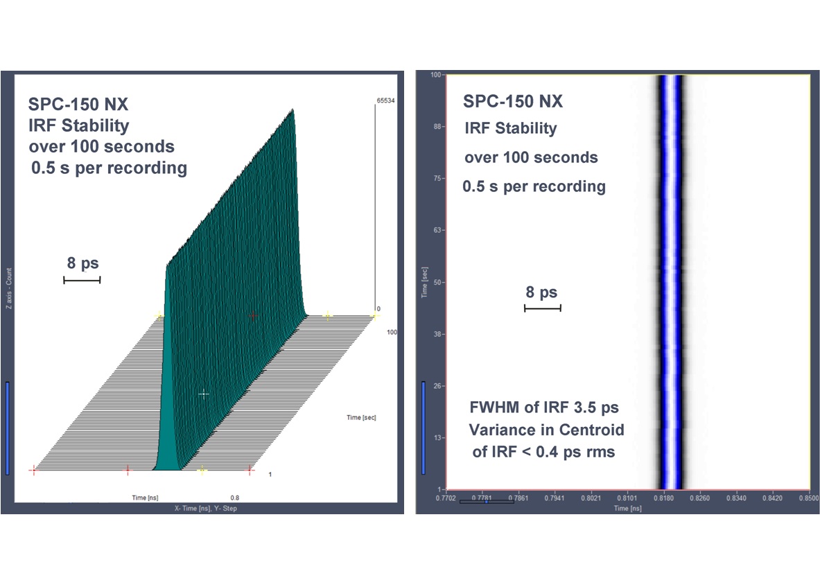
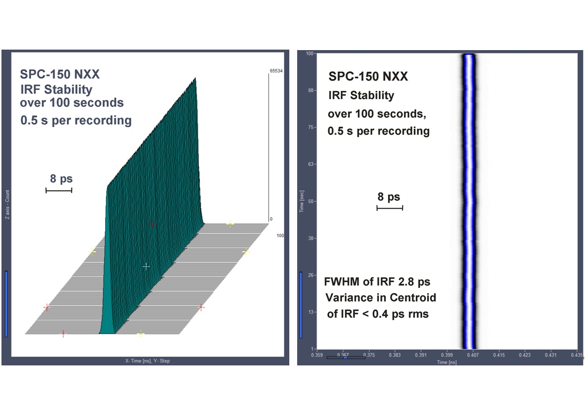
- Extremely High Timing Stability, Low-Frequency Timing Wobble < 0.4 ps RMS
- 10 MHz Saturated Count Rate
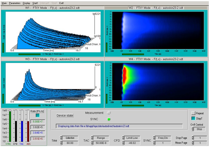
- Single Mode, Oscilloscope Mode, FLIM, PLIM, FLITS, FCS, Mosaic FLIM
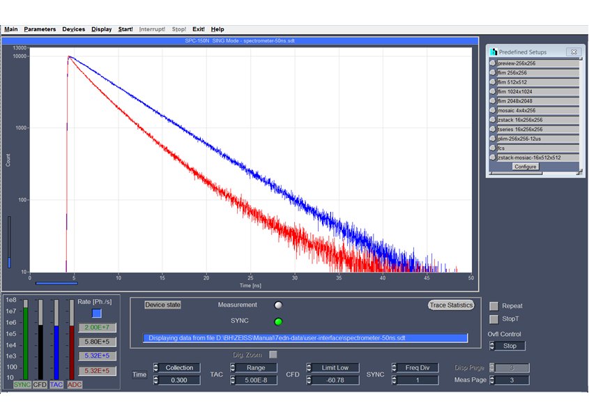
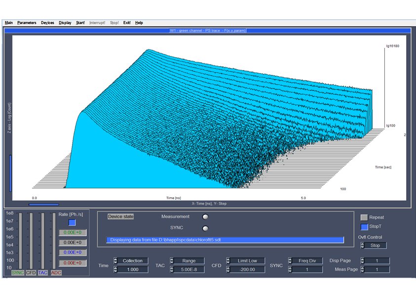
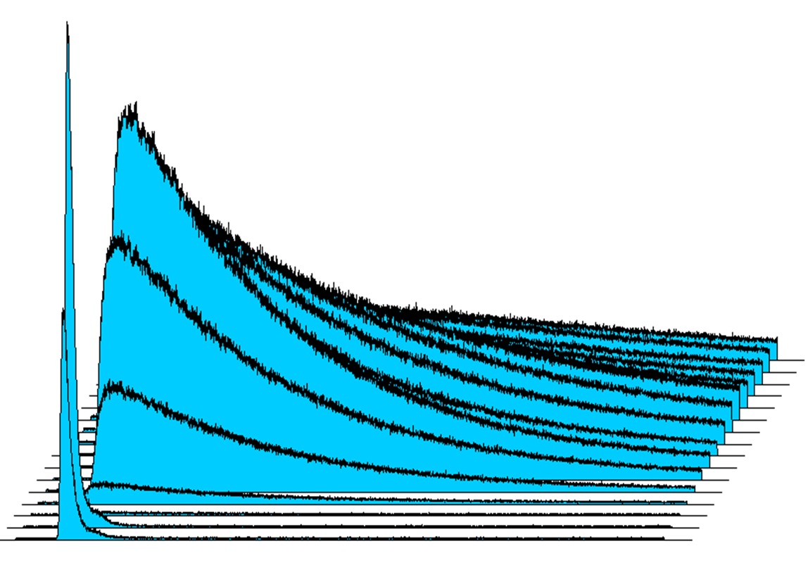
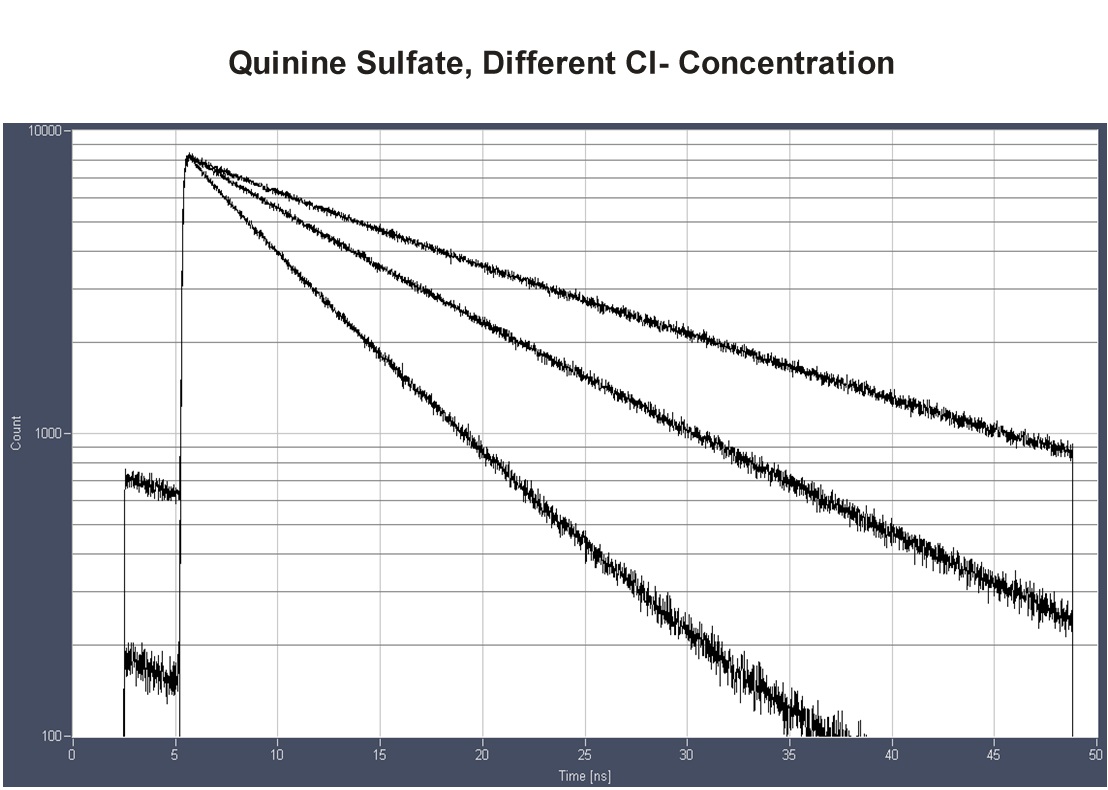
- Fluorescence Decay Recording
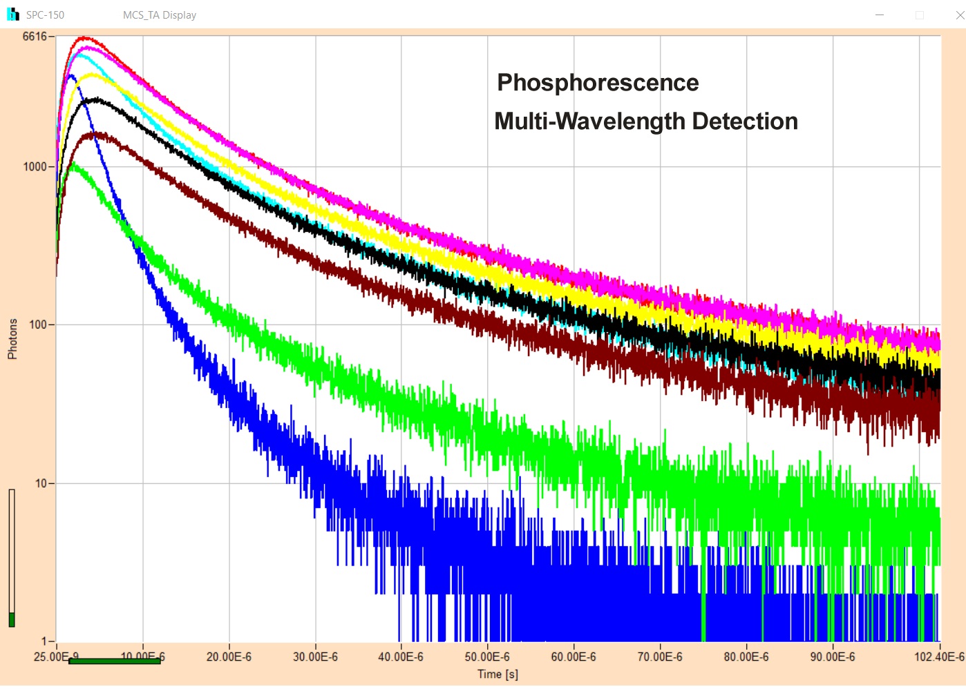
- Phosphorescence Decay Recording
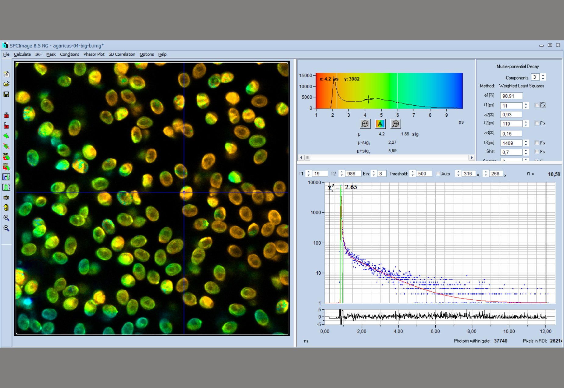
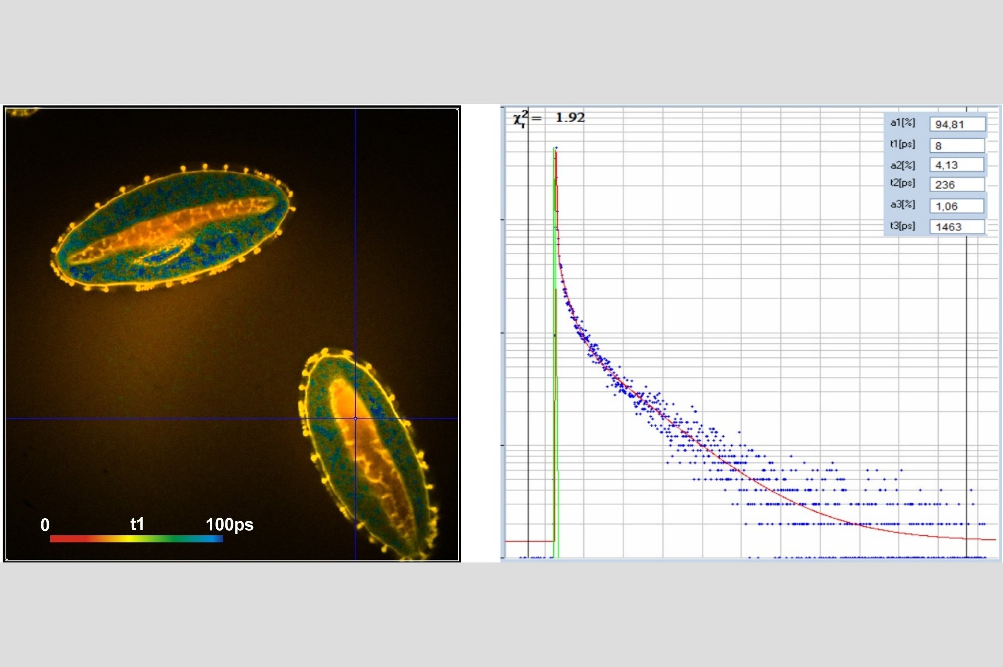
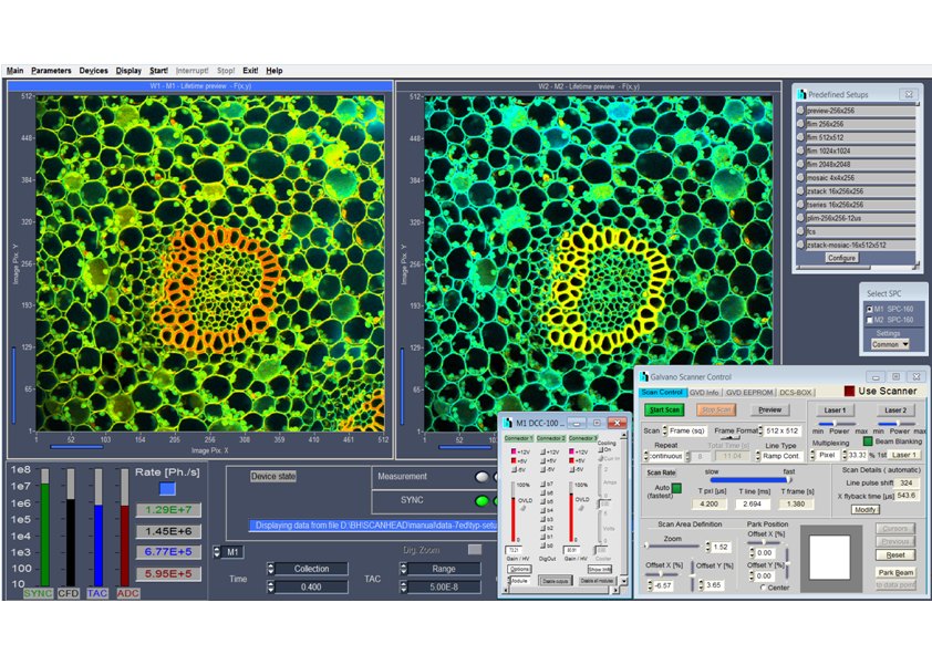
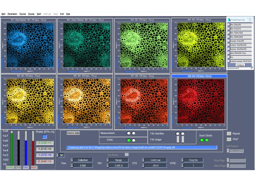
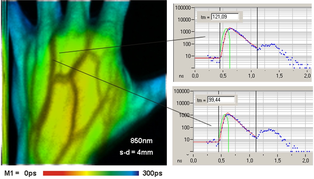
- Fluorescence and Phosphorescence Lifetime Imaging
- Photon Correlation
- Single-Molecule Spectroscopy
- Free Instrument Software for Windows 10 / 11 (Realtime Calculation and Fitting of FCS Curves)
- Parallel Operation of Up to 4 Modules
- Available as Multi-Module Package e.g. SPC-152N, SPC-153N and SPC-154N
Description
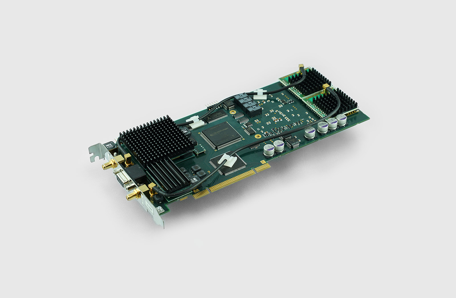
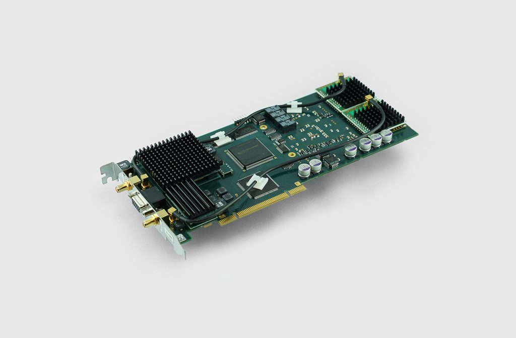
The SPC-150N is an all-purpose TCSPC and FLIM module with PCI bus interface. The board can be used for fluorescence lifetime measurements, single molecule spectroscopy, FCS and FCCS recording, FLIM, Mosaic FLIM, FLITS, and combined FLIM / PLIM applications.
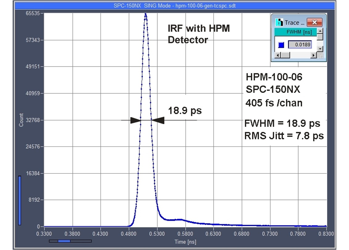
The SPC-150NX is a resolution-enhanced version of the SPC-150N for ultra-fast detectors. The board can be used for traditional fluorescence lifetime measurements, single molecule spectroscopy, FCS and FCCS recording, FLIM, Mosaic FLIM, FLITS, and combined FLIM / PLIM applications. The SPC-150NX is recommended especially for applications that require ultimate time resolution from superconducting detectors, MCP PMTs, and fast hybrid detectors.
General Information
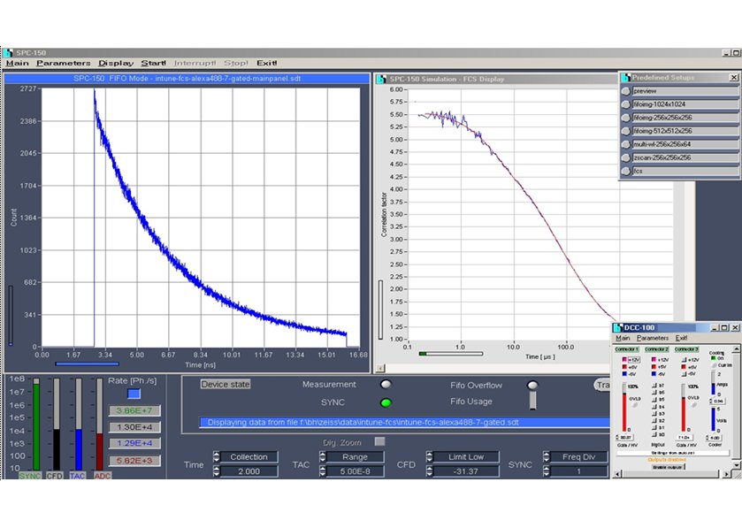
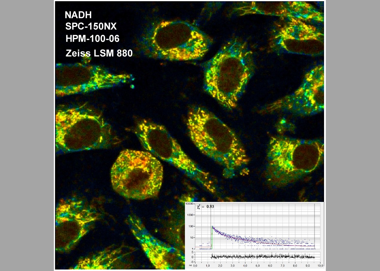
The SPC-150N boards have a large internal memory and a fast bus interface and ultra-fast discriminators in the detector- and synchronization inputs. This allows the modules to obtain superior time resolution with detectors that both have low transit time spread and an extremely fast single photon response. They are recommended especially for superconducting detectors, MCP PMTs, and fast hybrid detectors with bi-alkali or multi-alkali cathodes. They offer all standard photon distribution modes, the continuous-flow mode, the FIFO (time-tag) mode and the FIFO Imaging (FLIM) mode is implemented. The SPC-150N board can thus be used for traditional fluorescence lifetime experiments, diffuse optical tomography, stopped flow experiments, single molecule spectroscopy, FCS and FCCS recording, FLIM, Mosaic FLIM, FLITS, and combined FLIM / PLIM. One or more SPC-150N modules are used for the bh DCS-120 confocal FLIM system. They are also the basis of standard FLIM systems for the Zeiss LSM 710 and 510 microscopes and various other confocal and multiphoton laser scanning microscopes.
The SPC-150NX board is a resolution-enhanced version of the SPC-150N. The minimum time-channel width is 405 fs. These modules are recommended especially for applications that require ultimate time resolution from superconducting detectors, MCP PMTs, and fast hybrid detectors. The SPC-150NX achieves sub-20 ps (FWHM) IRF width with these detectors.
Measurement Software Included
The SPCM operating and measurement software is included with all SPC series modules. SPCM provides online calculation and display (2D, 3D) of data (decay curves, FLIM, FCCS) acquired in multiple operation modes. SPCM software undergoes active continuous development. SPCM receives frequent updates with new features and bug fixes. Read more…
FLIM and FCS Data Analysis
For advanced fluorescence lifetime imaging (FLIM) and single-curve data analysis, please use SPCImage.
For advanced fluorescence correlation spectroscopy (FCS) and cross-correlation (FCCS) data analysis, please use Burst Analyzer.
Custom Programming Libraries (DLL, LabVIEW)
For automation and custom software integration, DLLs and LabVIEW drivers are available. Read more…
Specifications
|
SPC-150N |
SPC-150NX |
SPC-150NXX |
|||
|
Photon Channel |
|
||||
|
Principle |
Constant Fraction Discriminator (CFD) |
||||
|
Discriminator Input Bandwidth |
4 GHz |
||||
|
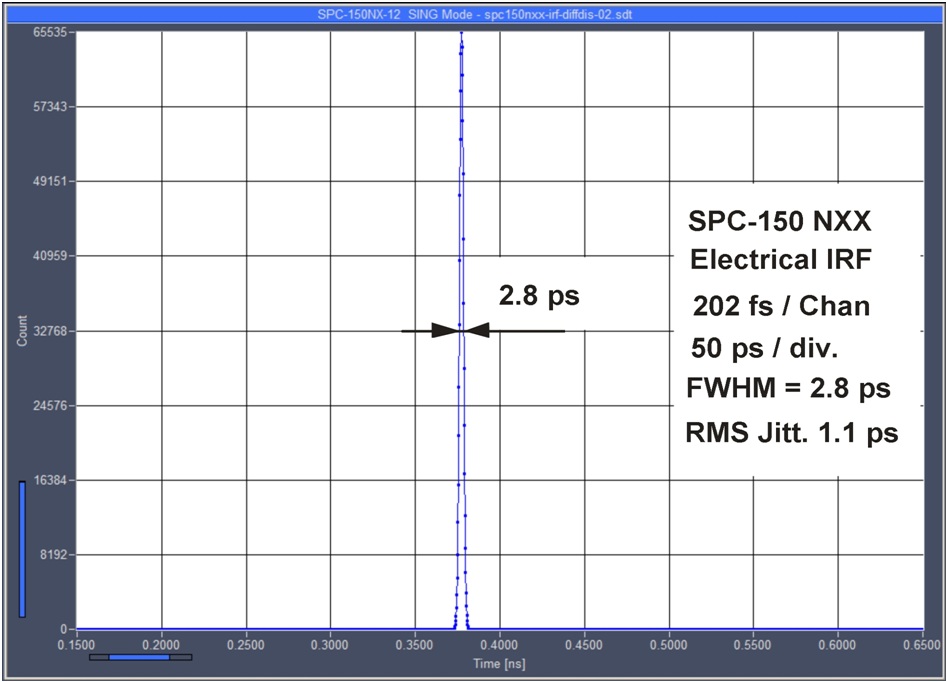
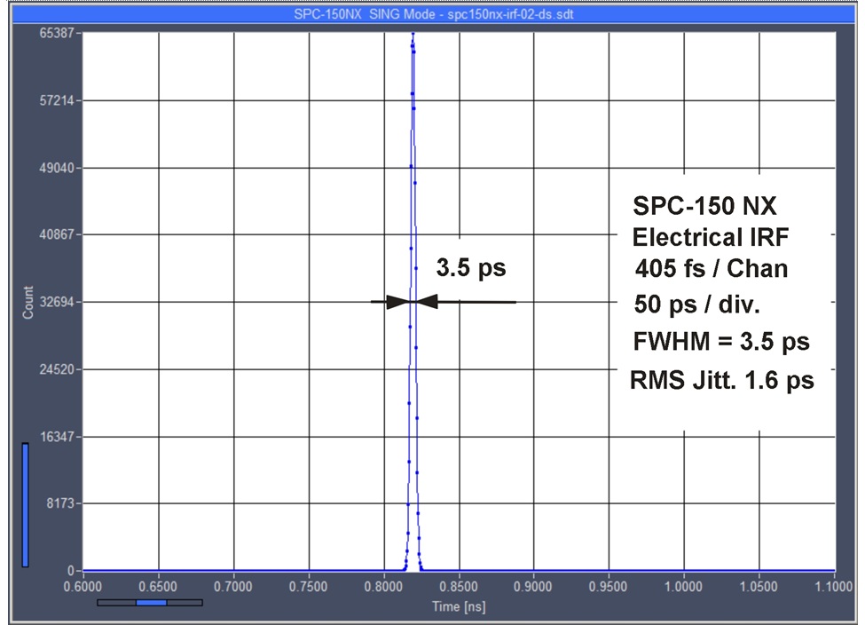
Time Resolution (FWHM/RMS, electr.) |
6.6 ps / 2.5 ps |
< 3.5 ps / 1.6 ps |
< 3 ps / 1.1 ps |
||
|
Variance in Time of IRF max. (RMS) |
< 1 ps over 50 s |
< 0.4 ps over 100 s |
< 0.4 ps over 100 s |
||
|
Optimum Input Voltage Range |
-30 mV to -500 mV |
||||
|
Min. Input Pulse Width |
200 ps |
||||
|
Threshold |
0 to -250 mV |
||||
|
Zero Cross Adjust |
-100 mV to 100 mV |
||||
|
Syncronisation Channel |
|
||||
|
Principle |
Constant Fraction Discriminator (CFD) |
||||
|
Discriminator Input Bandwidth |
4 GHz |
||||
|
Optimum Input Voltage Range |
-30 mV to -500 mV |
||||
|
Min. Input Pulse Width |
200 ps |
||||
|
Threshold |
0 to -250 mV |
||||
|
Frequency Range |
0 to 150 MHz |
||||
|
Frequency Divider |
1, 2, 4 |
||||
|
Zero Cross Adjust |
-100 mV to 100 mV |
||||
|
Time-to-Amplitude Converters / ADCs |
|
||||
|
Principle |
Ramp Generator / Biased Amplifier |
||||
|
TAC Range |
50 ns to 5 µs |
25 ns to 2.5 µs |
12.5 ns to 50 ns |
||
|
Biased Amplifier Gain |
1 to 15 |
||||
|
Biased Amplifier Offset (of TAC Range) |
0 % to 100 % |
0 % to 50 % |
0 % to 50 % |
||
|
Time Range incl. Biased Amplifier |
3.3 ns to 5 µs |
1.67 ns to 2.5 µs |
0.834 ns to 50 ns |
||
|
Min. Time Channel Width |
813 fs |
407 fs |
203 fs |
||
|
ADC Principle |
50 ns Flash ADC with Error Correction |
||||
|
Diff. Nonlinerarity |
< 0.5 % RMS, typ. < 1 % peak-peak |
||||
|
Data Acquisition |
Histogram Mode |
||||
|
Method |
on-board multi-dim. histogramming process |
||||
|
Dead Time |
100 ns, independent of computer speed |
||||
|
Saturated Count Rate |
10 MHz |
||||
|
Useful Count Rate |
5 MHz |
10 MHz |
|||
|
Max. Counts / Time Channel |
16 bits |
||||
|
Overflow Control |
none, stop, repeat and correct |
||||
|
Collection Time |
0.1 µs to 100,000 s |
||||
|
Diplay Interval Time |
0.1 µs to 100,000 s |
10 ms to 100,000 s |
|||
|
Repeat Time |
0.1 µs to 100,000 s |
||||
|
Sequencing Recording |
Programmable Hardware Sequencer, unlimited recording by Memory swapping, in curve mode and scan mode |
||||
|
Syncronisation with Scanning |
Pixel, Line and Frame from Scanning Device |
||||
|
Input Count Enable Control |
1 bit, TTL |
||||
|
Input Experiment Trigger |
TTL |
||||
|
Data Acquisition |
FIFO / Parameter-Tag Mode |
||||
|
Method |
Time and wavelength tagging of individual photons and continuous writing to disk |
||||
|
Online Display |
Decay functions, FCS, Cross-FCS, PCH MCS Traces |
||||
|
FCS Calculation |
Multi-tau algorithm, online calculation and online fit |
||||
|
Number of counts of decay/ waveform recording |
unlimited |
||||
|
Dead Time |
100 ns |
||||
|
Saturated Count Rate, Peak |
10 MHz |
||||
|
Sustained Count Rate (bus transfer limit) |
typ. 4 MHz |
||||
|
Output Data Format (ADC / Macrotime / Routing) |
12 / 12 / 4 |
||||
|
FIFO Buffer Capacity (Photons) |
2 * 106 |
||||
|
Macro Timer Resolution, Internal Clock |
25 ns, 12 bit, overflows marked by MOTF entry in data stream |
||||
|
Input Macro Timer Resolution, Clock from Sync |
10 ns to 100 ns, 12 bit, overflow marked by MOTF entry in data stream |
||||
|
Input Curve Control (external Routing) |
4 bit, TTL |
||||
|
External Event Markers |
4 bit, TTL |
||||
|
Input Count Enable Control |
1 bit, TTL |
||||
|
Input Experiment Trigger |
TTL |
||||
|
Data Acquisition |
FIFO / Parameter-Tag Imaging Mode |
||||
|
Method |
Buildingup images from time- and wavelength tagged data |
||||
|
Online Display |
up to 8 Images in different time and wavelength windows |
||||
|
Synchronisation with Scanner |
via Frame Clock, Line Clock and Pixel Clock Pulses |
||||
|
Detector / Wavelength Channels |
1 to 16 |
||||
|
Image resolution (64-bit SPCM Software) |
|
||||
|
No. of Time Channels |
64 |
256 |
1024 |
4096 |
|
|
No. of Pixels, 1 Detector Channel |
4096 x 4096 |
2048 x 2048 |
1024 x 1024 |
512 x 512 |
|
|
No. of Pixels, 16 Detector Channels |
1024 x 1024 |
512 x 512 |
256 x 256 |
128 x 128 |
|
|
Operation Environment |
|
||||
|
PC System |
Windows 8 / 10, > 8 GB RAM, 64 bit operating system recommended |
||||
|
PC Interface |
PCI |
||||
|
Power Consumption |
approx. 12 W from +5 V, 0.7 W from +12 V |
||||
|
Dimensions |
240 mm x 130 mm x 15 mm |
||||
Downloads
Documents
Datasheets
Applications
- STED FLIM
- Ophthalmic FLIM (FLIO)
- In Vivo FLIM of Skin
- Fluorescence Correlation – FCS
- Full Correlation Down to Picoseconds
- Antibunching Experiments by TCSPC
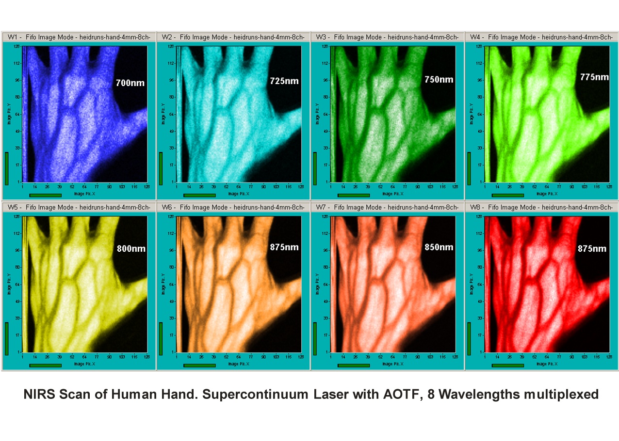
- NIRS
- fNIRS
- DCS – Diffuse Correlation
- Classic TCSPC
- Multidimensional TCSPC
- TCSPC FLIM
- Multi-Wavelength FLIM
- Simultaneous FLIM / PLIM
- Fluorescence Cross Correlation – FCCS
Application Notes
- Two-Photon Fluorescence Excitation by Picosecond Diode Lasers
- Time-Tag Recording: A New Old Feature of the bh SPC Cards
- FLIM in the FIFO Imaging Mode: Large Images with Small TCSPC Modules
- Non-Descanned FLIM Systems for Olympus FV-1000 and FV-300 Multiphoton Microscopes
- Recording the Instrument Response Function of a Multiphoton FLIM System
- Recording Z Scans with the DCS-120 Confocal Scanning FLIM System
- Tuneable Excitation FLIM with the LSM 710 Intune System
- An 8-Channel Parallel Multispectral TCSPC FLIM System
- Microsecond Decay FLIM: Combined Fluorescence and Phosphorescence Lifetime Imaging
- Spatially Resolved Recording of Fluorescence-Lifetime Transients by Line- Scanning TCSPC
- Combined Fluorescence and Phosphorescence Lifetime Imaging (FLIM / PLIM) with the Zeiss LSM 710 NLO Microscopes
- TCSPC at Wavelengths from 900 nm to 1700 nm
- FLIM and FCS by Pulse-Interleaved Excitation with the Zeiss LSM 710/780 Intune System
- Mosaic FLIM: New Dimensions in Fluorescence Lifetime Imaging
- Zeiss BiG-2 GaAsP Detector is Compatible with bh FLIM Systems
- NSOM FLIM with the Nanonics AFM/NSOM System
- Implantable Fibre-Optical Fluorescence-Lifetime Detection System for in-vivo Applications
- TCSPC Fibre-Probe System with an Exchangeable Tip
- bh FLIM Systems Record Calcium Transients in Live Neurons
- The PZ-FLIM-110 Piezo-Scanning FLIM System
- 80 ps FHWM Instrument Response with ID230 InGaAs SPAD and SPC-150 TCSPC Module
- bh – Abberior Combination Records STED FLIM at Megapixel Resolution
- SPCM Software Runs Online-FLIM at 10 Images per Second
- bh TCSPC Systems Record FLIM with Sutter MOM Microscopes
- Wide-Field TCSPC FLIM with bh SPC-150N TCSPC System and Photek FGN 392-1000 Detector
- Ultra-fast HPM Detectors Improve NAD(P)H FLIM
- TCSPC System Records FLIM of a Rotating Object
- Shifted-Component Model Improves FLIO Data Analysis
- 273 ps FWHM TCSPC Response with Hamamatsu H15620 NIR PMT
- An AFM/NSOM System with Fluorescence Lifetime Imaging
- Fast-Acquisition TCSPC FLIM System with sub-25 ps IRF Width
- Metabolic FLIM of Macroscopic Objects
- Suppression of Lens Fluorescence in FLIO Images of Cataract Patients
- 8.7 ps FWHM IRF Width from Ultrafast SPAD
- A Differential Discriminator for bh TCSPC Modules
- Influence of Magnetic Fields on the IRF of High-Speed Detectors for TCSPC
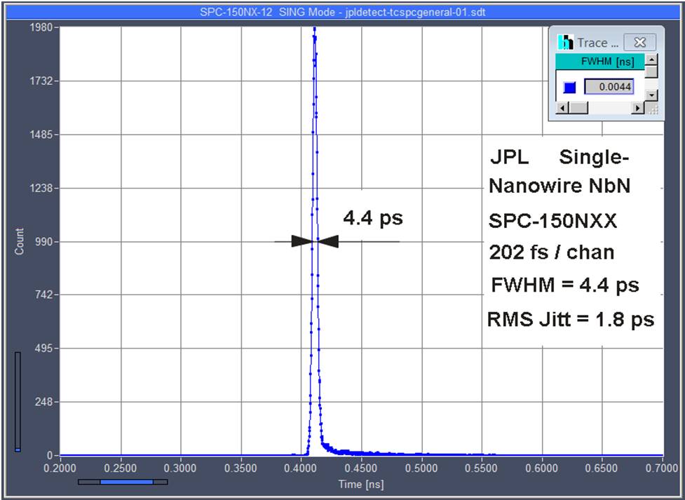
- 4.4 ps IRF width of TCSPC with an NbN Superconducting Nanowire Single Photon Detector
- Fast-Acquisition TCSPC FLIM: What are the Options?
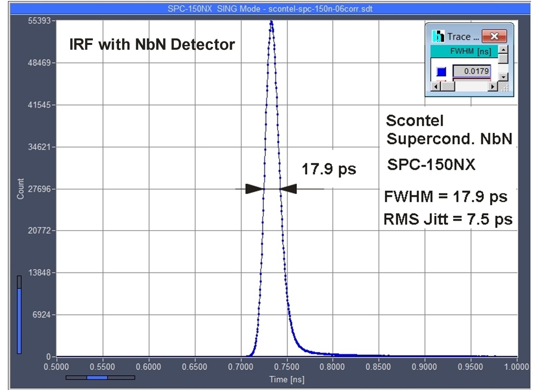
- World Record in TCSPC Time Resolution: Combination of bh SPC-150NX with SCONTEL NbN Detector yields 17.8 ps FWHM
Principles
The bh SPC modules use a multi-dimensional TCSPC principle. The principle is an extension of the classic TCSPC process: A detector detects single photons of a periodic light signal. The TCSPC electronics measures the times of the photons within the signal (excitation) period, and builds up the distribution of the photons over the time of the signal period. The time resolution of the TCSPC process is much higher than the resolution of an analog recording with the same detector: The time of a photon pulse can be determined with a much higher precision than its width.
In extension of the classic process, the bh technique determines additional parameters of the photons, such as wavelength, point of origin within an image area, excitation wavelength, time from an external stimulation of the sample, time within an additional modulation period of the excitation light. The photon distribution is built up over the photon times in the signal period and one or several of these additional parameters. The results of this process are multi-wavelength fluorescence-decay data, fluorescence-lifetime images, multi-wavelength lifetime images, multi-excitation decay data or multi-excitation FLIM data, decay data or FLIM data of fast dynamic changes within a sample, or combined fluorescence / phosphorescence decay data or FLIM / PLIM data. Please see also 'The bh TCSPC Technique'.
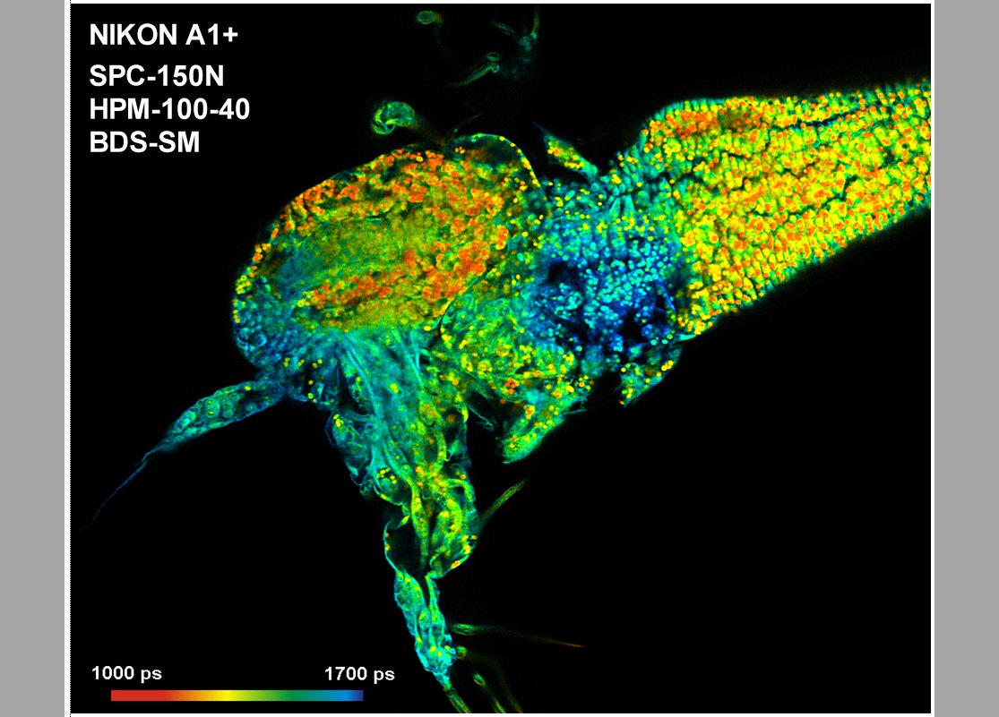
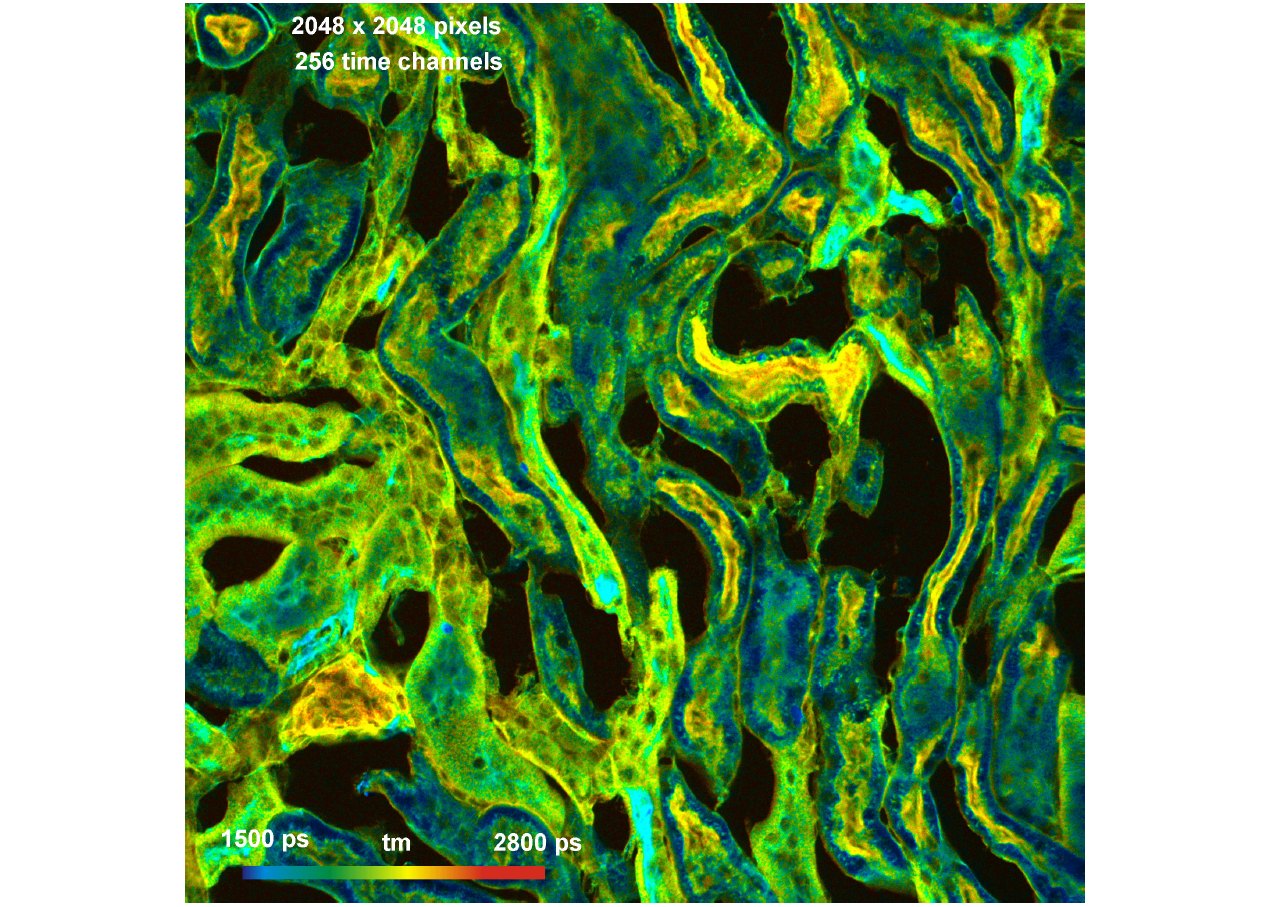
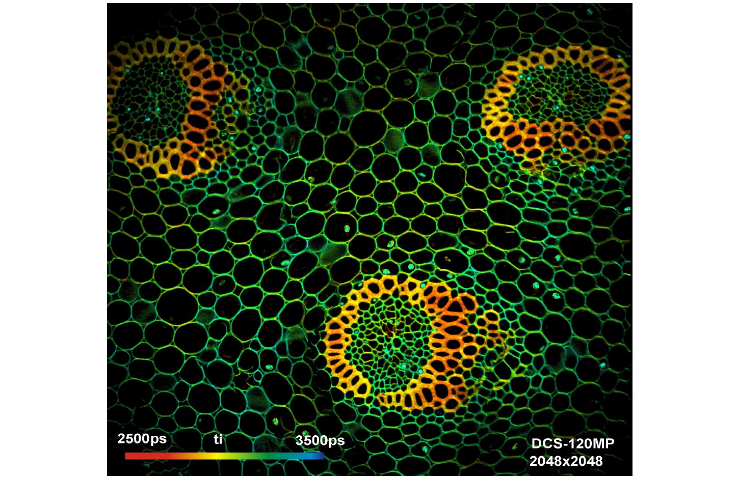
Gallery